Product
NEMST-Waterfall2008 或Matrix2008
Atmospheric Plasma Cleaner_Water
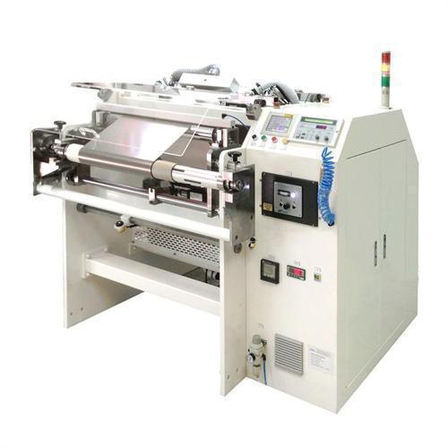
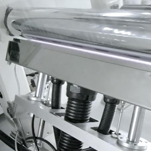
- Plasma Electrode will be installed above the roller with film.
- Dielectric Barrier Discharge (DBD) Plasma Electrodes Design.
- Direct or In-direct/Remote Plasma Design.
- Electrode width can be designed based on customers' requirements.
- Electrodes can be expanded with higher treatment speed.
- Reel-to-Reel Plasma Treatment.
- Single Side Plasma Treatment.
- Reaction Gases: CDA or N2. Low Gas and Electricity Running Costs.
- Plasma Effective Width: 100 mm ~ 2300 mm. (Can be larger based on customers' requirements).
- Treatment Speed: 0.5 ~ 10 m / min in general (Can be changed based on customers' requirements).
- High Plasma Treatment Stability and Uniformity.
- Surface Cleaning and Surface Modifications for Flexible PCB Panels before Gold Plating, Copper Plating or Shipping.
- Suitable for Film Treatment For Touch Panel or Optoelectronics Applications.
- Electronic and Non-electronics Devices Plasma Treatment With Metal or Non-Metal Materials. (e.g. PI, PET, PE, Plastic).
- Film Growth Applications.